


By using THz spintronic emission, we could study the spin-charge conversion mechanisms in 2D materials. High crystalline quality 2D materials are grown by molecular beam epitaxy on large area and CoFeB is deposited on top using soft UHV sputtering to obtain sharp interfaces. Such model system allows us to identify and quantify the spin-charge conversion mechanisms in 2D PtSe2
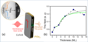

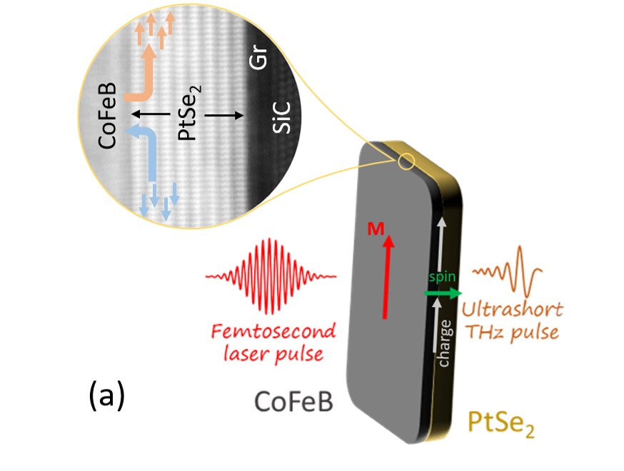
a: Schematics of THz spintronic emission from the CoFeB/PtSe2 bilayer. An atomic scale scanning transmission electron microscopy image shows the material stacking with high quality interfaces. The photoexcitation and diffusion of spin up and down generate a pure spin current perpendicular to the film and a charge current parallel to the film. B: Intensity of the THz electric field as a function of PtSe2 thickness (in ML) showing two regimes for thin (<4 ML) and thick (>4 ML) PtSe2. Blue dots are experimental data and solid lines fits using a simple spin diffusion model.
THz spintronic emission is based on the ultra-rapid conversion of a spin current into a charge current providing an intense, broadband source of THz waves. It is a formidable tool for the fundamental study of spin-to-charge conversion mechanisms in materials. Here, we have used this technique to study the spintronic properties of 2D materials. Indeed, by studying this emission according to the nature, symmetry and number of layers of the 2D material, it is possible to identify the spin-charge conversion mechanisms in theory and practice, and to quantify them. However, this kind of study is limited by two major obstacles: the growth of high quality 2D materials over large areas, and the control of the interface between the 2D material and the ferromagnet used as the spin current source. Today, 2D materials are mostly studied in the form of micrometric flakes mechanically exfoliated from the bulk material. Moreover, the interface between 2D materials and metallic ferromagnets shows chemical reactions and atomic interdiffusion. In this work, we have overcome these two obstacles to study spin-charge conversion mechanisms in 2D PtSe2 exhibiting an electronic transition from the semiconductor to the semi-metallic state by increasing the number of monolayers (ML). Large area single crystalline PtSe2 was grown by molecular beam epitaxy and CoFeB was then deposited in the same chamber under ultra-high vacuum by soft sputtering giving high quality interface. To identify conversion mechanisms and quantify them, THz spintronic emission was used as illustrated (a). This technique is highly sensitive and non-destructive. Among 2D materials, PtSe2 exhibits an intense THz signal, making it possible to study emission as a function of the number of ML (b). At low thicknesses (<4 ML), in the semiconductor regime, charge transfer between the graphene substrate and the first layer of PtSe2 creates an interface electric field and a strong Rashba effect responsible for spin-charge conversion by the inverse Rashba-Edelstein effect and the THz signal. This is an interface effect. For thicker layers (>4 ML), the transition to the semi-metallic state adds the inverse spin-Hall effect conversion phenomenon, which corresponds to a volume effect. Theoretical studies using a simple spin diffusion model and ab initio calculations have validated this interpretation and quantified these effects. 2D materials open up new horizons for the development of tunable THz spintronic emitters in a sustainable way.
Teams: 2D spintronics, Theory and Simulations
Collaboration: IRIG-MEM/SYMMES/PHELIQS, LPENS (Paris), LAF (Palaiseau), C2N (Palaiseau), NEEL (Grenoble)
Funding: Equipex + 2D-MAG
Further reading: K. Abdukayumov et al., Atomic-Layer Controlled Transition from Inverse Rashba–Edelstein Effect to Inverse Spin Hall Effect in 2D PtSe2 Probed by THz Spintronic Emission. Adv. Mater. 2024, 36, 2304243. https://doi.org/10.1002/adma.202304243
Contact: Matthieu Jamais, Mairbek Chshiev