Post-doctoral position available at IRIG/Spintec (12 months with possible extension)
Nanostructures of 2D Materials for quantum optics and spintronics (NanoDRUM project)
Recently, there has been tremendous interest in layered transition metal dichalcogenides (TMDCs). It started with the discovery that the canonical TMDC MoS2 becomes a direct bandgap semiconductor when isolated in monolayer (ML) form [Splendiani et al., Nano Lett. 10, 1271 (2010), Mak et al., Phys. Rev. Lett. 105, 136805 (2010)]. Their spectrally narrow photoluminescence and absorption make them very good candidates for novel optoelectronic devices. The combination of a bandgap and an atomically thin conducting channel also makes TMDCs ideal materials for next generation field effect transistors in microelectronics [Radisavljevic et al., Nat. Nanotechnol. 6, 147 (2011)]. Finally, in the monolayer form, due to the breaking of inversion symmetry and strong spin-orbit coupling, the carriers in TMDCs carry a valley index noted K+ or K-. This valley degree of freedom can be exploited to develop novel spintronic/valleytronic devices [Zeng et al., Nat. Nanotechnol. 7, 490 (2012)]. However the integration of these materials into real devices raises several challenges that our Institute is currently addressing: the growth of TMDCs on large areas, their transfer onto suitable substrates (to limit the interaction with the TMDC) and perform optical and electrical measurements. The Physics department of IRIG at the CEA Grenoble (including Spintec, MEM and PHELIQS labs) wants to strengthen its activities in two specific topics based on the use of TMDC layers: quantum optics and spintronics.
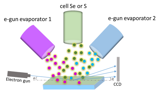
In the context of the NanoDRUM project, the postdoc will be first in charge of the growth of TMDC layers (MoSe2 and WSe2) on insulating substrates (SiO2, sapphire, mica and hBN) over 1 cm2 by van der Waals epitaxy in a dedicated molecular beam epitaxy (MBE) machine. He will then investigate the optical (photoluminescence and absorption) and electrical (doping, mobility) of as-grown TMDC layers. In a second step, he will develop the most suitable method (dry, wet or by SmartCutTM) to transfer the TMDC layers onto a pre-patterned SiO2/Si substrate and preserve the electronic properties of the TMDC. The pre-patterned SiO2/Si substrate will consist of nano-holes in the SiO2 layer in order to obtain suspended TMDC membranes and test their individual optical properties like the emission of single photons. In a possible extended period, the postdoc will integrate suspended TMDC layers into simple spintronic devices to study spin/valley transport and compare it with supported layers.
The postdoc will work in collaboration with the CEA/LETI for layer transfer and the fabrication of pre-patterned SiO2/Si substrates, the PFNC at Minatec for structural and electronic characterizations and the Néel Institute for optical measurements.
Requirements: Good experience in MBE, TMDC physics (optics and/or spintronics), TMDC layer transfer, electron beam lithography for the fabrication of patterned SiO2/Si substrates and to contact the TMDC layers for electrical measurements.
Starting: Fall 2019, duration 12 months (possible extension to 18 months)
Contacts:
- At IRIG/Spintec: Matthieu Jamet, tel. +33-438782262 (office) / +33-620081119 (mobile)
- At IRIG/MEM: François Rieutord, Hanako Okuno
- At IRIG/PHELIQS: Jean-Michel Gérard

