Overview
Materials development is a fundamental activity at SPINTEC, a determining factor for the success of our research projects. The Materials Growth team assists and participates on the development and characterization of new materials and stacks for the different research projects. Sputtering and molecular beam epitaxy (MBE) are our two main deposition techniques. The team also maintains our tools at the best operational order and upgrades them to keep them at the state of the art.
Most of our research teams depend on our sputtering facilities, capable of depositing a wide range of metals, rare earths and oxides in an industrially friendly fashion. We currently have two tools in operation (ACTEMIUM and PLASSYS) and a third one under construction in-house (Convergence).
Techniques and equipments
ACTEMIUM – Sputtering

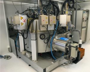
ACTEMIUM is our main tool with 12 sputtering sources under very high vacuum (10-8 mbar) capable of DC and RF excitation for conducting and isolating targets. In this tool, a separate treatment chamber allows us to plasma clean the substrates prior to deposition or to oxidize films by exposing them to oxygen with a possible plasma assistance. This tool allows us to deposit extremely complex stacks with up to dozens of individual films and thicknesses down to 0.1 nm. Common stacks include MgO insulating barriers for magnetic tunneling junctions (MTJ), Pt/Co multilayers with perpendicular anisotropy, and synthetic antiferromagnetic stacks with RKKY coupling.
Convergence – Sputtering

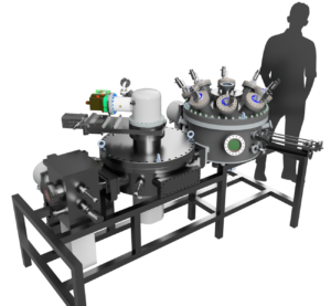
Convergence is a new UHV sputtering tool under construction in-house that will be dedicated to the development of new materials, with shorter campaigns than with our other tools. The design consists on three chambers: load-lock, distribution and deposition chamber, the latter with 8 convergent sources. Simplicity and modularity are the main features of this machine, that will be able to evolve over time with ports reserved for two additional chambers and an exchangeable sample holder.
Annealing

Annealing is a fundamental step in most of our stacks. We anneal routinely to pin a ferromagnetic layer in a given direction with an adjacent antiferromagnetic layer or to crystallize amorphous films. We are equipped with a MATr 2000 200mm oven capable of applying a magnetic field of up to 2 T, a rapid thermal annealing 100 mm oven, and a small sample oven with up to 0.2 T field.
Current in plane tunneling

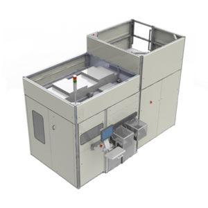
Magnetic tunnel junctions (MTJ) are basic building blocks of many of our stacks. After deposition, a quick feedback on their properties is key for a fast development cycle. The CAPRES CIPT tool allow us to measure the tunneling magneto resistance (TMR) without the need of time-consuming nanofabrication procedures.
Molecular Beam Epitaxy

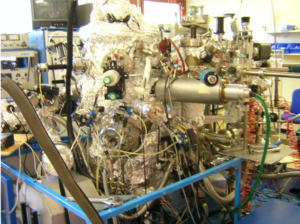
We use a custom-made cluster for the growth of transition metal dichalcogenides (TMDC) and topological insulators (TI). The UHV cluster is equipped with 2 Kundsen cells, 11 crucibles for e-beam evaporation, 4 sputtering sources and a sample holder capable of heating up to 1300 K. RHEED characterization is possible during growth. With this tool we are able to create 2D systems at the interface between two films.
The team
Recent news
- Sub-10nm thermally stable Perpendicular Shape Anisotropy STT-MRAM realized at SPINTEC (March 08th, 2018)

A team at SPINTEC in Grenoble has demonstrated thermally stable and electrically switchable Spin Transfer Torque MRAM (STT-MRAM) of diameter down to 4nm. Among the various technologies of non-volatile memories, STT-MRAM gathers a unique combination ... - Enhanced annealing stability and perpendicular magnetic anisotropy in perpendicular magnetic tunnel junctions using W layer (November 15th, 2017)

The stiffening of the perpendicular magnetic tunnel junction (pMTJ) stack resulting from the W insertion due to its very high melting temperature, is the key mechanism behind the extremely high thermal robustness. Thicker W layer ... - Spin-Hall Voltage over a Large Length Scale in Bulk Germanium (July 20th, 2017)

Germanium is one of the most appealing candidate for spintronic applications, thanks to its compatibility with the Si platform, the long electron spin lifetime and the optical properties matching the conventional telecommunication window. Electrical spin ... - Nanotweezers and their remote actuation by magnetic fields (May 23rd, 2017)

We have developed arrays of innovative magnetic nanotweezers or “nanojaws” on silicon wafers, by a top-down approach using the fabrication techniques of microelectronics. The mechanical manipulation of micro- and nanometric objects relies on constantly evolving techniques, ... - Millimeter-scale layered MoSe2 grown on sapphire and evidence for negative magnetoresistance (April 14th, 2017)

We have fabricated large-scale two-dimensional transition metal dichalcogenide (2D TMD) MoSe2, a promising candidate for electronics, valley-spintronics and optoelectronics, on insulating sapphire and have investigated its structural and transport properties. We have shown that the ...


