Overview
Materials development is a fundamental activity at SPINTEC, a determining factor for the success of our research projects. The Materials Growth team assists and participates on the development and characterization of new materials and stacks for the different research projects. Sputtering and molecular beam epitaxy (MBE) are our two main deposition techniques. The team also maintains our tools at the best operational order and upgrades them to keep them at the state of the art.
Most of our research teams depend on our sputtering facilities, capable of depositing a wide range of metals, rare earths and oxides in an industrially friendly fashion. We currently have two tools in operation (ACTEMIUM and PLASSYS) and a third one under construction in-house (Convergence).
Techniques and equipments
ACTEMIUM – Sputtering
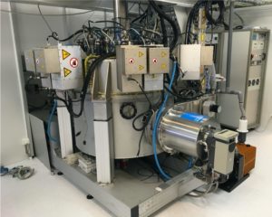
ACTEMIUM is our main tool with 12 sputtering sources under very high vacuum (10-8 mbar) capable of DC and RF excitation for conducting and isolating targets. In this tool, a separate treatment chamber allows us to plasma clean the substrates prior to deposition or to oxidize films by exposing them to oxygen with a possible plasma assistance. This tool allows us to deposit extremely complex stacks with up to dozens of individual films and thicknesses down to 0.1 nm. Common stacks include MgO insulating barriers for magnetic tunneling junctions (MTJ), Pt/Co multilayers with perpendicular anisotropy, and synthetic antiferromagnetic stacks with RKKY coupling.
Convergence – Sputtering
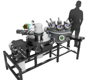
Convergence is a new UHV sputtering tool under construction in-house that will be dedicated to the development of new materials, with shorter campaigns than with our other tools. The design consists on three chambers: load-lock, distribution and deposition chamber, the latter with 8 convergent sources. Simplicity and modularity are the main features of this machine, that will be able to evolve over time with ports reserved for two additional chambers and an exchangeable sample holder.
Annealing
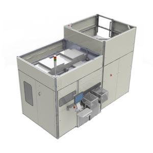
Annealing is a fundamental step in most of our stacks. We anneal routinely to pin a ferromagnetic layer in a given direction with an adjacent antiferromagnetic layer or to crystallize amorphous films. We are equipped with a MATr 2000 200mm oven capable of applying a magnetic field of up to 2 T, a rapid thermal annealing 100 mm oven, and a small sample oven with up to 0.2 T field.
Current in plane tunneling

Magnetic tunnel junctions (MTJ) are basic building blocks of many of our stacks. After deposition, a quick feedback on their properties is key for a fast development cycle. The CAPRES CIPT tool allow us to measure the tunneling magneto resistance (TMR) without the need of time-consuming nanofabrication procedures.
Molecular Beam Epitaxy
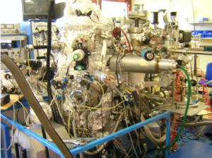
We use a custom-made cluster for the growth of transition metal dichalcogenides (TMDC) and topological insulators (TI). The UHV cluster is equipped with 2 Kundsen cells, 11 crucibles for e-beam evaporation, 4 sputtering sources and a sample holder capable of heating up to 1300 K. RHEED characterization is possible during growth. With this tool we are able to create 2D systems at the interface between two films.
The team
Recent news
- Self-induced spin-charge conversion in ferromagnetic thin films (February 28th, 2020)

The generation of a spin current and its further conversion to a charge current have attracted considerable attention, facilitating advances in basic physics along with the emergence of closely related applications in the field of ... - Spintronic memristor based on an isotropically coercive magnetic layer (December 03rd, 2019)

We propose an original concept of spintronic memristor based on the angular variation of the tunnel magnetoresistance (TMR) of a nanopillar comprising several magnetic layers. We have experimentally developed the appropriate magnetic free layer and ... - Impact of eddy currents in nanostructures destined for use in spintronics (September 11th, 2019)

In the field of spintronics, ferromagnetic/non-magnetic metallic multilayers are core building blocks for emerging technologies. Resonance experiments using stripline transducers are commonly used to characterize and engineer these stacks for applications. Here, we investigated the incompletely understood ... - Magnetic control of optical responses of biocompatible magneto-elastic membranes (August 29th, 2019)

Numerous studies investigated the use of synthetic membranes for photonic or biomedical applications. We report here on a recent type of biocompatible magnetically actuated membranes, partly originating from studies on magnetic particles for biology, consisting ... - Physicochemical origin of improved MRAM cells with W capping layer (August 20th, 2019)

Increasing the thermal budget beyond 400°C of magnetic random access memory (MRAM) cells is a major goal to allow for seamless conventional electronics integration. At these temperatures significant material diffusion can destroy the interface properties ...


