Objectives
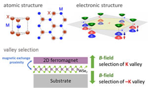
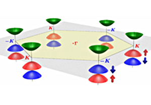
In the monolayer limit, two dimensional (2D) transition metal dichalcogenides (2H-MX2, with M=Mo, W and X=S, Se) are semiconductors with a sizeable (1-2 eV) and direct electronic bandgap as well as (degenerate) valleys at the K+/K- corners of the Brillouin zone. Beyond their use as classical semiconductors, this peculiar electronic structure opens new and exciting possibilities for information processing that exploit the quantum degree of freedom known as the valley index. This emergent field of research is known as « valleytronics ». It has been established that K+/K- valleys can be selectively addressed by using circularly polarized light and that the valley Hall effect allows resolving the valley polarization of charge carriers. However, for practical use of these materials in valleytronics, a means of reaching a permanent (and tunable) lifting of the valley degeneracy at K+ and K- has to be developed. The aim of the MAGICVALLEY project is to develop a new and promising method to reach this objective, which consists in breaking the time-reversal symmetry in MX2 through magnetic exchange coupling with a 2D (para)magnetic material.
First, efforts will be dedicated to the growth and to the extensive characterization of magnetic 2D layers which can be either a ferromagnetic 2D layer (VSe2, MnSe2) or MSe2 (M=Mo, W) layers doped with magnetic impurities. Then, magnetic 2D layer/MX2 van der Waals heterostructures will be developed to explore the valley polarization by magnetic exchange proximity. The materials will be grown over large areas (1 cm2) by molecular beam epitaxy and chemical vapor deposition. This approach will provide the ultraclean interfaces needed for an efficient exchange coupling. Moreover, using van de Waals bonded layers will largely suppress interface reactivity. The project involves a comprehensive set of characterization techniques to firmly establish the atomic, magnetic and electronic structures of the constituent materials. Finally, the splitting of the valleys, a key step for valleytronics, will be investigated by both optical spectroscopy and electrical measurements. The experimental work will be supported by an important theoretical effort. All the partners of the project have a strong expertise in the study of 2D materials in their own field.
Contacts in SPINTEC and INAC
JAMET Matthieu (Spintec), MARTY Alain (Spintec), VERGNAUD Céline (Spintec), BEIGNE Cyrille (Spintec), CHSHIEV Mair (Spintec), OKUNO Hanako (MEM), GREVIN Benjamin (SYMMES).
Other partners
- Institut NEEL, Grenoble, France. VEUILLEN Jean-Yves, MALLET Pierre, BOUKARI Hervé, GENUIST Yann, MAGAUD Laurence
- Laboratoire de Physique et Chimie des Nano-Objets, INSA, Toulouse, France. MARIE Xavier, RENUCCI Pierre, BALOCCHI Andrea, AMAND Thierry, URBASZEK Bernhard, HAN Bo, SHREE Shivanghi
- Centre de Nanosciences et Nanotechnologies, Marcoussis, France. OUERGHI Abdelkarim, MAILLY Dominique, CHASTE Julien, CAVANNA Antonella, GIRARD Jean-Christophe
Publications
[ At Spintec (default) | Entire consortium ]

