Integrated Circuits (ICs) have to be protected against threatening environmental radiations and malicious perturbations. A large panel of countermeasures have been developed to answer the needs of this challenging field. This work proposes an innovative sensor to detect both photoelectrical injections and thermal perturbations aiming a circuit. This architecture is designated by “Dual Detection of Heating and Photocurrent attacks (DDHP)”.
During the computation of a cryptographic algorithm, when faults are injected in specific locations of the IC and at the right time, it makes possible the retrieval of secret data. CMOS circuitry and Back-End of Line (BEoL) memories can both be sensitive to physical perturbations, by inducing a photocurrent in the structure or by heating it for instance. The Bulk Built-In Current Sensor (BBICS) is a widely studied detector enabling to sense any photocurrent induced in the bulk of a circuit. Such a sensor is efficient for integrated circuit back-side attacks.
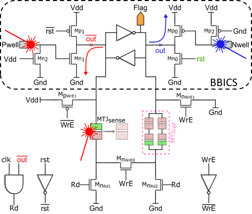
This work highlights the hybridization of this BBICS solution with the STT-MRAM technology in order to also sense front side thermal attacks. The proposed sensor is designated by “Dual Detection of Heating and Photocurrent attacks (DDHP)”. This countermeasure is illustrated in this figure.
The implementation of this sensor was realized using the 28 nm FD-SOI Process Design Kit combined to STT-MRAM junctions with a diameter of 40 nm. Electrical and Monte Carlo simulations have demonstrated the excellent efficiency of this detector while facing different attacks aiming the P-substrate, the N-well or the STT-MRAM junctions. The DDHP sensor detects all these attacks from both sides of the integrated circuit, to then communicate failures to the system. After each detection and depending on the application, the system has then to decide the operation to be achieved as for instance erasing all the data in the circuit or restarting from the last known and secured functional state.
The same structure was also developed in the 180 nm Bulk CMOS and 200 nm junction diameter technologies as part of the GREAT project and was taped out. Thus, an experimental work testing the scope of action in terms of area of detection of a DDHP sensor must be led and depending on the observations, an advanced DDHP structure could be proposed.
Team: Spintronics IC design
Collaboration: CEA tech (Gardanne), IM2NP – Aix Marseille University (Marseille), EMSE (Ecole des Mines de Saint-Etienne).
Funding: GREAT European project, MASTA ANR project.
Further reading: Dual Detection of Heating and Photocurrent attacks (DDHP) Sensor using Hybrid CMOS/STT-MRAM, M. Kharbouche-Harrari, R. Wacquez, G. Di Pendina, J.–M. Dutertre, J. Postel-Pellerin, D. Aboulkassimi and J-M. Portal, In 2019 IEEE 25th International Symposium on On-Line Testing And Robust System Design (IOLTS).
Contact: Gregory Di Pendina

Figure: Structure of the proposed DDHP sensor combining the BBICS sensor to STT-MRAM circuitry.


